Most of us in the MLOps world spend our days one or two layers above silicon — pipelines, GPUs-as-a-service, model serving, observability. It’s easy to treat the chip underneath as a black box that “just works.” But every argument we make about scaling AI in India — more inference, more fine-tuning, more sovereign models — eventually runs into a hard wall: how much compute exists, who controls its design, and what it costs. That wall is made of silicon, and right now it is being redrawn by an open standard called RISC-V.
This piece is for MLOps practitioners and for the wider professional audience who has never opened a chip datasheet — because the story is genuinely about all of us.
The RISC-V advantage: an instruction set nobody owns
RISC-V is an open instruction set architecture (ISA) — the vocabulary a processor understands. Unlike x86 (controlled by Intel and AMD) or Arm (licensed, fee-bearing, tightly gated), RISC-V is royalty-free and not owned by any single company or country. Anyone, anywhere, can build a processor on it without paying licensing fees or asking permission.
Three things follow from that, and they compound:
- It is genuinely modular. The base RISC-V instruction set has fewer than 100 instructions. Everything else — vector math, cryptography, custom AI acceleration — is an optional extension a designer can bolt on only if their workload needs it. A hearing-aid chip and a datacenter server chip can share the same root ISA while looking nothing alike internally.
- It permits real customisation. Companies can add proprietary instructions on top of the open base — something that is heavily restricted or outright forbidden on x86 and Arm. That is a level of hardware-software co-design that used to be reserved for a handful of hyperscalers with the deepest pockets.
- It is a genuinely multinational effort. Because no single nation or company gatekeeps it, RISC-V has attracted funding, contribution, and adoption from organisations and governments across the US, Europe, China, and India simultaneously. That breadth of investment is producing a pace of innovation that a single vendor’s closed roadmap struggles to match.
The net effect: the cost of building a competent, application-specific processor has fallen from hundreds of millions of dollars to, in some cases, tens of millions — because you no longer have to design an entire ISA and toolchain from scratch, and you aren’t paying a licensing toll on every unit you ship.
The architecture innovation: chiplets, and the standard that connects them
For most of computing history, a processor was one monolithic piece of silicon. That approach is running into physical and economic limits — bigger dies are harder to manufacture without defects, and cramming everything onto one chip means every function is stuck on the same, one-size-fits-all manufacturing process.
The industry’s answer is chiplets: instead of one giant chip, you build several smaller, specialised dies — a CPU chiplet here, a memory controller there, an AI accelerator elsewhere — manufactured independently, sometimes by different vendors, sometimes on different process nodes, and then packaged together as one system. It improves manufacturing yield, lets each function use the process node that suits it best, and — critically — lets you mix and match components instead of building everything in-house.
For chiplets to talk to each other, they need a common electrical and protocol language. That’s UCIe — Universal Chiplet Interconnect Express — an open die-to-die interconnect standard launched in 2022 and co-developed by AMD, Arm, Google Cloud, Intel, Meta, Microsoft, Qualcomm, Samsung, TSMC, and (as board members) Nvidia and Alibaba. UCIe does for chiplets roughly what USB did for peripherals: it lets a CPU chiplet from one vendor talk to an accelerator chiplet from a completely different vendor, inside the same package, at very high bandwidth.
RISC-V and UCIe are a natural pairing. Because RISC-V is open and license-free, it is an ideal candidate for the “known good die” CPU chiplet that anyone can drop into a UCIe-based package alongside their own custom accelerator — without having to license someone else’s proprietary core just to get a CPU into the mix.
How this is actually being used today
Inside a Google TPU or Meta MTIA-style package
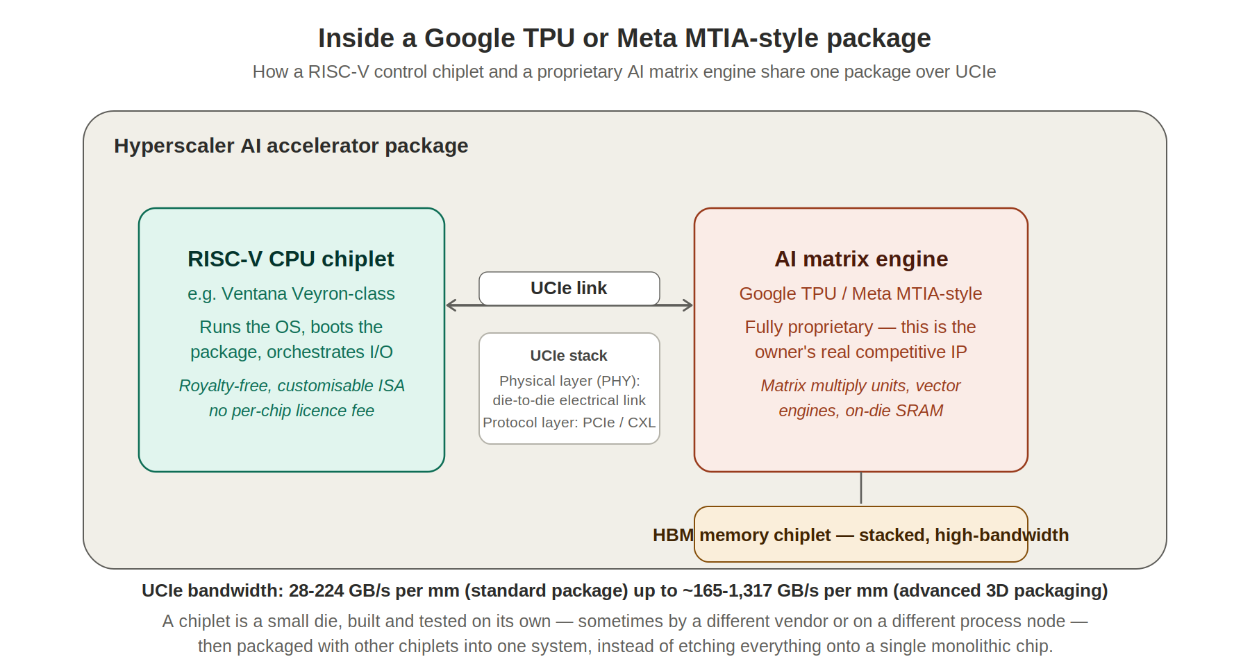
A RISC-V control chiplet and a proprietary AI matrix engine, wired together over UCIe
A chiplet, to be precise about it, is simply a small die — built, tested, and yield-checked on its own, sometimes by a different vendor or on a different manufacturing process — that gets combined with other chiplets inside a single package, instead of one team trying to etch an entire system onto one giant monolithic die. It’s the semiconductor industry’s version of modular construction: build the pieces separately, assemble them at the end, and swap out only the piece that needs to change.
Ventana Micro Systems sells its Veyron RISC-V CPU as exactly this kind of chiplet — a “known good die” a hyperscaler can pair with its own accelerator, memory, and I/O logic rather than standing up an entire CPU core design team. The latest Veyron generation supports up to 32 cores per chiplet, connects over UCIe, and includes the current RISC-V vector extension for AI workloads.
This is the pattern both Google’s TPU program and Meta’s MTIA program are built on: a fully proprietary AI matrix engine — the matrix-multiply units, vector engines, and on-die SRAM that represent the company’s actual competitive edge — sitting on the same package as a RISC-V control chiplet that boots the system, runs the OS, and orchestrates everything around it, all wired together over UCIe, with an HBM memory chiplet stacked alongside for bandwidth.
The UCIe link itself is worth understanding, because the numbers are startling: its die-to-die physical layer, built on PCIe and CXL protocol foundations, delivers roughly 28–224 GB/s per millimetre of die edge in a standard package, and up to somewhere in the 165–1,317 GB/s per millimetre range in advanced 3D packaging — a 20x to 100x-plus improvement over a standard PCIe link. That bandwidth is precisely what makes it viable to split a chip into separately-designed pieces without paying a crippling performance tax for the privilege.
It’s worth noting Ventana itself was reportedly the subject of an acquisition move by Qualcomm earlier this year — a sign of how seriously established chipmakers now take this space.
The RISC-V core hiding inside every NVIDIA Blackwell-class GPU
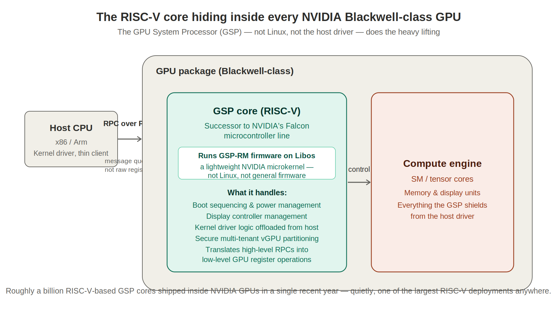
The GPU System Processor (GSP): not Linux, not the host driver — it does the heavy lifting
Even Nvidia — the company most associated with proprietary, closed-architecture silicon — has quietly built RISC-V into the heart of its GPUs since the Turing generation, and it carries straight through into Blackwell-era parts. It’s called the GPU System Processor (GSP), and it’s a genuinely clever piece of engineering hiding in plain sight.
The GSP is the successor to Nvidia’s earlier Falcon line of embedded microcontrollers, now rebuilt on a RISC-V core. Crucially, it does not run Linux, and it isn’t just executing raw assembly the way the old Falcon “ucode” did either — it runs Nvidia’s own firmware, called GSP-RM (a GPU-resident version of the driver’s Resource Manager), on top of a small, purpose-built microkernel Nvidia calls Libos. That’s a deliberate choice: a general-purpose OS would be too heavy and too slow to boot for a component that has to come alive before almost anything else on the card does. For the most security-sensitive configurations, Nvidia has even built a formally verified separation-kernel variant, written in Ada/SPARK, to isolate GPU partitions between untrusted tenants.
What does the GSP actually take off the host CPU’s plate? A great deal: boot sequencing and power management, display controller management, and — the big one — the low-level kernel driver logic itself. Instead of the host talking directly to hundreds of individual GPU control registers, it sends a high-level command over a message-queue RPC channel to the GSP, which translates that into the actual low-level register operations, manages memory and display controllers, and enables use cases like secure multi-tenant vGPU sharing in the cloud, where a hypervisor hands a slice of the GPU to a guest VM with the GSP enforcing the isolation. Nvidia has said it shipped roughly a billion RISC-V cores in a single recent year through this and similar embedded uses — a genuinely enormous, and largely invisible, RISC-V deployment.
Why this matters right now: compute sovereignty is not theoretical anymore
A few weeks ago, the US government issued an export control directive forcing Anthropic to disable access to its most capable model tier — Mythos and Fable — for all foreign nationals, everywhere, including Anthropic’s own non-US employees. The directive wasn’t aimed at India specifically; it applied globally. But it made something concrete that had mostly been discussed in the abstract: access to frontier AI capability can be switched off overnight by a decision made entirely outside the country using it, for reasons that don’t have to be fully disclosed even to the company involved.
Whatever one thinks of the specific merits of that decision, it’s a useful jolt for anyone building AI infrastructure outside the US. It underlines a point that applies just as much to hardware as to models: if the compute your AI/MLOps stack depends on is designed under someone else’s export licence, someone else’s national interest ultimately sits upstream of your roadmap. RISC-V’s royalty-free, cross-national nature is the one part of the modern compute stack genuinely insulated from that dynamic — nobody can revoke your right to use an ISA nobody owns.
India already has a seat at this table
This isn’t a hypothetical opportunity — India has been building toward it for close to a decade, and it deserves more visibility than it gets:
- The SHAKTI processor program at IIT Madras, one of the founding contributors to the RISC-V Foundation itself, has been developing indigenous RISC-V cores since 2013, including an aerospace-grade chip developed jointly with ISRO — designed, fabricated, packaged, and booted entirely within India.
- InCore Semiconductors, a Chennai-based startup spun out of the SHAKTI project and backed by PeakXV Partners (formerly Sequoia India), sells configurable RISC-V core generators rather than a fixed catalogue of cores — letting clients get a tailor-made processor instead of a one-size-fits-all part. It has already secured design wins internationally, including in aerospace and automotive.
- C-DAC’s VEGA RISC-V processor family, under the government’s Digital India RISC-V (DIRV) initiative, is already shipping in mass-market products like hearing aids and is the basis for at least one upcoming fully indigenous networking SoC.
- At Semicon India 2025, multiple Indian startups — working on everything from surveillance SoCs to motor-control ASICs for ISRO — showed RISC-V-based test chips taped out and headed for commercial production in 2026.
India reportedly already does 30–40% of the world’s chip design work, largely for other companies’ silicon. RISC-V’s openness is what turns that design capability into the ability to own the resulting IP outright, rather than renting it from an ISA licensor abroad. That is a meaningfully different economic position to be in.
What this means for MLOps practice, specifically
It’s tempting to file all of this under “hardware, not my problem.” I’d push back on that. Chiplets and UCIe are, in effect, an industrial-scale answer to a supply chain problem: they let more players design competitive silicon faster and cheaper, because nobody has to build every layer of the stack from a blank sheet. That accelerates the supply of GPUs, DPUs, and AI accelerators industry-wide.
For most of the last few years, the binding constraint on AI/MLOps adoption in India hasn’t been demand — teams everywhere want to run more models, more experiments, more inference. It’s been price and availability of compute. A more open, more competitive, more modular hardware supply chain — with India positioned as a design participant rather than purely a design-for-hire vendor — is one of the more credible paths to closing that gap over the next several years. Cheaper, more available accelerators don’t just help hyperscalers; they lower the floor for every MLOps team, startup, and researcher trying to get GPU-hours at a price that makes sense.
The conclusion I keep coming back to
RISC-V didn’t set out to be a geopolitical hedge — it set out to be a well-designed, open instruction set. But in a moment where access to frontier AI capability can be revoked by a directive issued 5:21pm on a Friday, the fact that nobody owns the ISA underneath your compute stack stops being a nice-to-have and starts looking like infrastructure resilience.
India has genuine, demonstrated capability here — SHAKTI, InCore, C-DAC’s VEGA, ISRO’s own indigenous chip work — and it sits inside a country that already does a disproportionate share of the world’s chip design labour. The chiplet era, standardised on open interconnects like UCIe, is lowering the capital and expertise bar to compete in silicon at exactly the moment India has the design talent to make use of it. The opportunity isn’t just to keep designing other people’s chips faster. It’s to design, package, and eventually manufacture more of our own — and in doing so, help solve the supply-side problem that’s been quietly capping how far AI and MLOps adoption can go in this country.
That’s a conversation worth having across our community — not just among chip engineers, but among everyone building the AI stack on top of them.
Sources consulted: UCIe Consortium, Wikipedia, and Semiconductor Engineering on UCIe bandwidth; SemiAnalysis, The Register, and ServeTheHome coverage of Ventana Veyron; RISC-V International, Nvidia’s open-gpu-kernel-modules documentation, and Linux kernel/nova-core documentation on the GPU System Processor and Libos; Anthropic’s public statement and Fortune/Al Jazeera reporting on the Fable/Mythos export control directive; InCore Semiconductors, RISC-V International, IIT Madras, and industry coverage of India’s SHAKTI, C-DAC VEGA, and DIRV initiatives.